Home /
Expert Answers /
Electrical Engineering /
welcome-to-cmos-layout-you-need-to-do-layout-for-a-part-of-the-mirror-adder-cell-as-shown-in-the-pa707
(Solved): Welcome to CMOS layout! You need to do layout for a part of the mirror adder cell, as shown in the ...
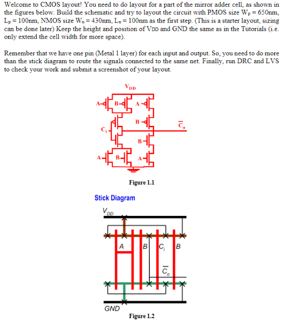
Welcome to CMOS layout! You need to do layout for a part of the mirror adder cell, as shown in the figures below. Build the schematic and try to layout the circuit with PMOS size W? = 650nm, Lp = 100nm, NMOS size W? = 430nm, L? = 100nm as the first step. (This is a starter layout, sizing can be done later) Keep the height and position of VDD and GND the same as in the Tutorials (i.e. only extend the cell width for more space). Remember that we have one pin (Metal 1 layer) for each input and output. So, you need to do more than the stick diagram to route the signals connected to the same net. Finally, run DRC and LVS to check your work and submit a screenshot of your layout. VDD C? B GND B Figure 1.1 Stick Diagram A BC B Figure 1.2 10? C