Home /
Expert Answers /
Electrical Engineering /
step-1-half-adder-design-the-half-adder-adds-two-1-bit-binary-inputs-a-and-b-it-generates-two-ou-pa433
(Solved): Step 1. Half Adder Design The half adder adds two 1-bit binary inputs a and b. It generates two ou ...
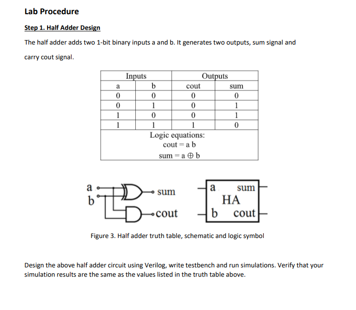
Step 1. Half Adder Design The half adder adds two 1-bit binary inputs a and b. It generates two outputs, sum signal and carry cout signal. Figure 3. Half adder truth table, schematic and logic symbol Design the above half adder circuit using Verilog, write testbench and run simulations. Verify that your simulation results are the same as the values listed in the truth table above.
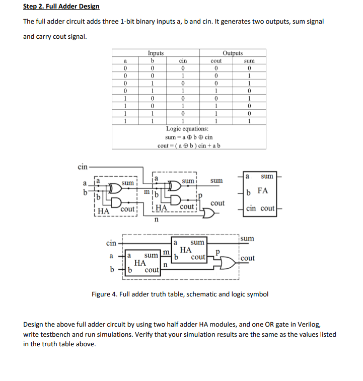
Step 2. Full Adder Design The full adder circuit adds three 1-bit binary inputs a, b and cin. It generates two outputs, sum signal and carry cout signal. Design the above tull adder c?rcuit by us?ng two halt adder HA modules, and one UK gate in Verilog, write testbench and run simulations. Verify that your simulation results are the same as the values listed in the truth table above.
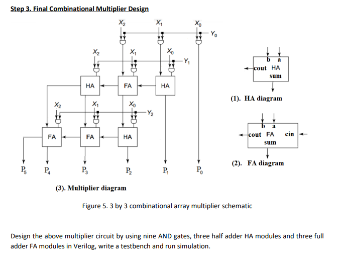
Step 3. Final Combinational Multiplier Design (1). HA diagram Figure \( 5.3 \) by 3 combinational array multiplier schematic Design the above multiplier circuit by using nine AND gates, three half adder HA modules and three full adder FA modules in Verilog, write a testbench and run simulation.
Expert Answer
Ans : Step 3:. module ha(i1,i2,s,c); input i1,i2; output s,c; assign s=i1^i2; assign c=i1&i2; endmodule module fa(i1,i2,cin,s,c); input i1,i2,cin; out


