Home /
Expert Answers /
Electrical Engineering /
question-5-a-what-is-the-capacitance-of-a-mos-diode-in-inversion-if-the-silicon-dioxide-thickne-pa759
(Solved): Question 5. (a) What is the capacitance of a MOS diode in inversion if the silicon dioxide thickne ...
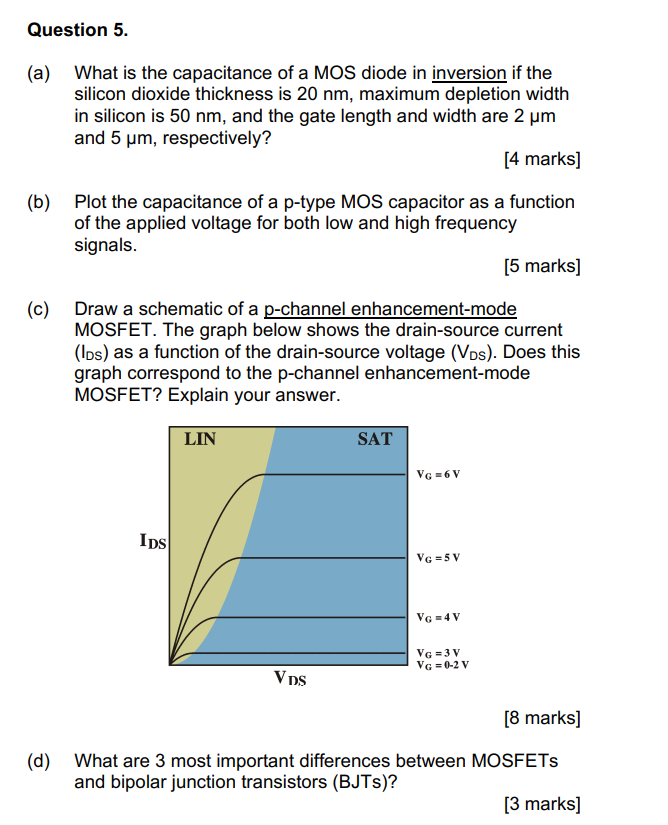
Question 5. (a) What is the capacitance of a MOS diode in inversion if the silicon dioxide thickness is 20 nm, maximum depletion width in silicon is 50 nm, and the gate length and width are 2 um and 5 um, respectively? [4 marks] (b) Plot the capacitance of a p-type MOS capacitor as a function of the applied voltage for both low and high frequency signals. [5 marks] (c) Draw a schematic of a p-channel enhancement-mode MOSFET. The graph below shows the drain-source current (lds) as a function of the drain-source voltage (Vos). Does this graph correspond to the p-channel enhancement-mode MOSFET? Explain your answer. LIN SAT VG =6V IDS VG = 5 V VG = 4V VG = 3 V VG = 0-2 V VDS [8 marks] (d) What are 3 most important differences between MOSFETS and bipolar junction transistors (BJTs)? [3 marks]