Home /
Expert Answers /
Electrical Engineering /
professional-of-computer-architecture-please-provide-the-complete-verilog-code-thank-you-lab-4-pa176
(Solved): Professional of Computer Architecture. Please provide the complete Verilog code. Thank you LAB 4: ...
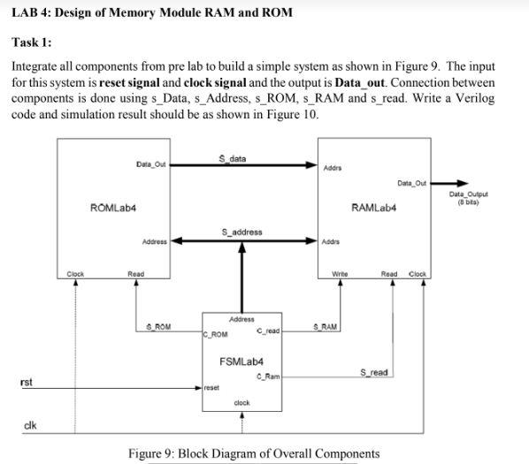
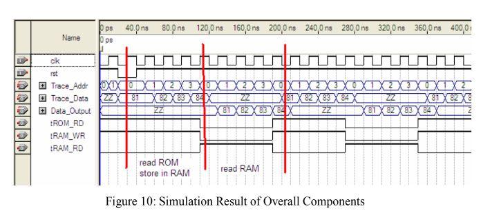
LAB 4: Design of Memory Module RAM and ROM Task 1: Integrate all components from pre lab to build a simple system as shown in Figure 9. The input for this system is reset signal and clock signal and the output is Data_out. Connection between components is done using s_Data, s_Address, s_ROM, s_RAM and s_read. Write a Verilog code and simulation result should be as shown in Figure 10. S data Data Out Addrs Data Out Data Output (8 bits) ROMLab4 S_address Address rst clk Clock Address Read ROM CROM Cread FSMLab4 C_Ram Addrs Write SRAM RAMLab4 Read S_read reset clock Figure 9: Block Diagram of Overall Components Clock
11000000 Name cik rst Trace_Addr Trace Data Data Output tROM_RD tRAM_WR tRAM_RD ps 40.0 ms 80.0 ns 120,0 ns 160,0 ns 200,0 ns 240,0 ns 280,0 ms 320,0 ms 360,0 ns 400,0 ps ??? XIXX1 X2 X3X0X1XEXE ZZX 81 X82X8384X 1000000 TOODET ZZ 81 82 83 84 ZZ X81X82X8 ZZ 81 82 83 84 ZZ 81 82 83 84 read ROM read RAM store in RAM Figure 10: Simulation Result of Overall Components