Home /
Expert Answers /
Electrical Engineering /
one-of-the-application-for-rlc-circuit-is-signal-filtering-signal-filtering-is-a-process-of-filte-pa186
(Solved): One of the application for RLC circuit is signal filtering. Signal filtering is a process of filte ...
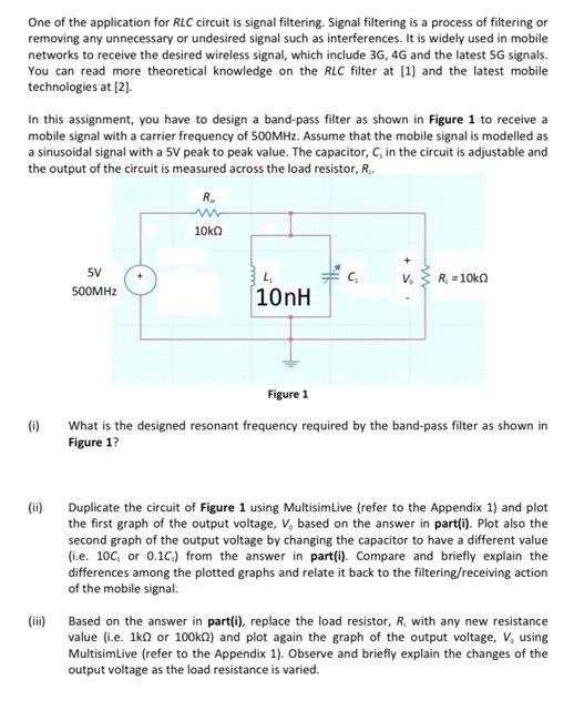
One of the application for RLC circuit is signal filtering. Signal filtering is a process of filtering or removing any unnecessary or undesired signal such as interferences. It is widely used in mobile networks to receive the desired wireless signal, which include \( 3 \mathrm{G}, 4 \mathrm{G} \) and the latest \( 5 \mathrm{G} \) signals. You can read more theoretical knowledge on the RLC filter at [1] and the latest mobile technologies at [2]. In this assignment, you have to design a band-pass filter as shown in Figure 1 to receive a mobile signal with a carrier frequency of \( 500 \mathrm{MHz} \). Assume that the mobile signal is modelled as a sinusoidal signal with a \( 5 \mathrm{~V} \) peak to peak value. The capacitor, \( C_{1} \) in the circuit is adjustable and the output of the circuit is measured across the load resistor, \( R_{\mathrm{b}} \). (i) What is the designed resonant frequency required by the band-pass filter as shown in Figure 1 ? (ii) Duplicate the circuit of Figure 1 using MultisimLive (refer to the Appendix 1) and plot the first graph of the output voltage, \( V_{0} \) based on the answer in part(i). Plot also the second graph of the output voltage by changing the capacitor to have a different value (i.e. \( 10 C_{1} \) or \( 0.1 C_{1} \) ) from the answer in part(i). Compare and briefly explain the differences among the plotted graphs and relate it back to the filtering/receiving action of the mobile signal. (iii) Based on the answer in part(i), replace the load resistor, \( R_{L} \) with any new resistance value (i.e. \( 1 \mathrm{k} \Omega \) or \( 100 \mathrm{k} \Omega \) ) and plot again the graph of the output voltage, \( V_{0} \) using MultisimLive (refer to the Appendix 1). Observe and briefly explain the changes of the output voltage as the load resistance is varied.
Expert Answer
you have any doubts, feel free to comment in the comment section.Thank you Answer 1) Circuit REF2 V2 VTN + REF2 R1 1 VL + REFI 1ko 10k? 27°C 1MHz V1 v
