Home /
Expert Answers /
Electrical Engineering /
on-the-band-diagram-below-a-bias-is-applied-across-the-semiconductor-of-length-mathrm-l-1-m-pa149
(Solved): On the band diagram below, a bias is applied across the semiconductor of length \( \mathrm{L}=1 \m ...
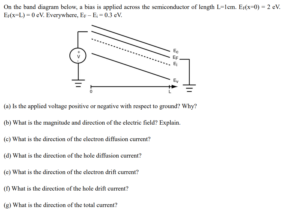
On the band diagram below, a bias is applied across the semiconductor of length \( \mathrm{L}=1 \mathrm{~cm} . \mathrm{E}_{\mathrm{F}}(\mathrm{x}=0)=2 \mathrm{eV} \). \( \mathrm{E}_{\mathrm{F}}(\mathrm{x}=\mathrm{L})=0 \mathrm{eV} \). Everywhere, \( \mathrm{E}_{\mathrm{F}}-\mathrm{E}_{\mathrm{i}}=0.3 \mathrm{eV} \). (a) Is the applied voltage positive or negative with respect to ground? Why? (b) What is the magnitude and direction of the electric field? Explain. (c) What is the direction of the electron diffusion current? (d) What is the direction of the hole diffusion current? (e) What is the direction of the electron drift current? (f) What is the direction of the hole drift current? (g) What is the direction of the total current?
