(Solved): In the following CMOS inverter logic gate, assume the transistor size of ((W)/(L))_(n)=0.8\mu (m)/(0 ...
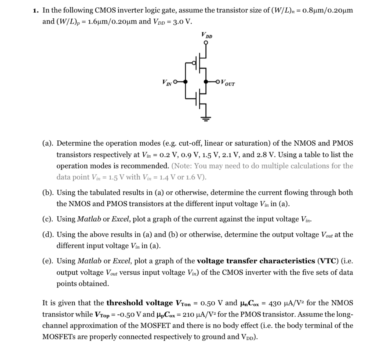
In the following CMOS inverter logic gate, assume the transistor size of
((W)/(L))_(n)=0.8\mu (m)/(0.20)\mu mand
((W)/(L))_(p)=1.6\mu (m)/(0.20)\mu mand
V_(DD)=3.0V. (a). Determine the operation modes (e.g. cut-off, linear or saturation) of the NMOS and PMOS transistors respectively at
V_(in )=0.2V,0.9V,1.5V,2.1V, and 2.8 V . Using a table to list the operation modes is recommended. (Note: You may need to do multiple calculations for the data point
V_(in )=1.5Vwith
V_(in )=1.4Vor 1.6 V ). (b). Using the tabulated results in (a) or otherwise, determine the current flowing through both the NMOS and PMOS transistors at the different input voltage
V_(in )in (a). (c). Using Matlab or Excel, plot a graph of the current against the input voltage
V_(in ). (d). Using the above results in (a) and (b) or otherwise, determine the output voltage
V_(out )at the different input voltage
V_(in )in (a). (e). Using Matlab or Excel, plot a graph of the voltage transfer characteristics (VTC) (i.e. output voltage
V_(out )versus input voltage
V_(in )) of the CMOS inverter with the five sets of data points obtained. It is given that the threshold voltage
V_(Ton )=0.50Vand
\mu _(n)C_(ox)=430\mu (A)/(V^(2))for the NMOS transistor while
V_(Top)=-0.50Vand
\mu _(p)C_(ox)=210\mu (A)/(V^(2))for the PMOS transistor. Assume the longchannel approximation of the MOSFET and there is no body effect (i.e. the body terminal of the MOSFETs are properly connected respectively to ground and
V_(DD)).