Home /
Expert Answers /
Electrical Engineering /
design-the-jfet-circuit-for-the-largest-i-d-swing-use-the-self-bias-circuit-shown-in-pa679
(Solved): Design the JFET circuit for the largest \( i_{D} \) swing. Use the self-bias circuit shown in ...
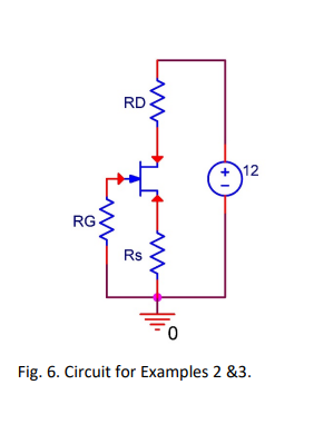
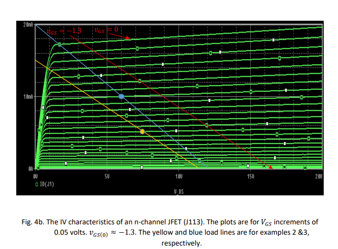
Design the JFET circuit for the largest \( i_{D} \) swing. Use the self-bias circuit shown in Fig. 6. Assume that \( v_{G S(0)}=-1.3 \) and \( V_{c c}=15 \) volts. Furthermore, assume that \( i_{D S S}=20 \mathrm{~mA} \). Using Fig. 4b, draw the load line and identify the Q point. Explain why this will allow the largest swing. Use \( i_{D}=i_{D S S}\left(1-\frac{v_{G S}}{v_{G S(0)}}\right)^{2} \) to show what happens to \( i_{D} \) and \( v_{D S} \) when you have a swing of \( 0.2 \) volts in \( v_{G S} \) form its operating point (that is, change \( v_{G S} \) by \( \pm 0.2 \) volts and compute the corresponding \( i_{D} \) and \( \left.v_{D S}\right) \)
Fig. 6. Circuit for Examples \( 2 \& 3 \).
Fig. 4b. The IV characteristics of an n-channel JFET (J113). The plots are for \( V_{G S} \) increments of \( 0.05 \) volts. \( v_{G S(0)} \approx-1.3 \). The yellow and blue load lines are for examples \( 2 \& 3 \), respectively.


