Home /
Expert Answers /
Electrical Engineering /
can-you-explain-the-answer-step-by-step-nbsp-part-i-part-ii-the-n-channel-enhancement-type-si-mosf-pa963
(Solved): can you explain the answer step by step part(i),part(ii) The N-channel enhancement type Si MOSF ...
can you explain the answer step by step
part(i),part(ii)


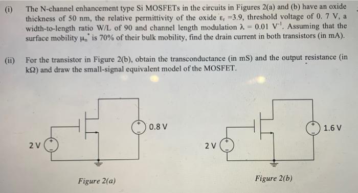
The N-channel enhancement type Si MOSFETs in the circuits in Figures 2(a) and (b) have an oxide thickness of \( 50 \mathrm{~nm} \), the relative permittivity of the oxide \( \varepsilon_{t}=3.9 \), threshold voltage of \( 0.7 \mathrm{~V} \), a width-to-length ratio \( \mathrm{W} / \mathrm{L} \) of 90 and channel length modulation \( \lambda=0.01 \mathrm{~V}^{-1} \). Assuming that the surface mobility \( \mu_{n}^{*} \) is \( 70 \% \) of their bulk mobility, find the drain current in both transistors (in mA). ii) For the transistor in Figure 2(b), obtain the transconductance (in \( \mathrm{mS} \) ) and the output resistance (in \( \mathrm{k} \Omega \) ) and draw the small-signal equivalent model of the MOSFET. Figure 2(a) Figure 2(b)