Home /
Expert Answers /
Computer Science /
and-this-is-figure-1-1-use-the-new-d-flip-flop-in-figure-1-and-design-a-4-bit-scalable-bit-sliced-pa966
(Solved): And this is figure 1 1. Use the new D Flip-Flop in Figure 1 and design a 4-bit scalable bit-sliced ...
And this is figure 1
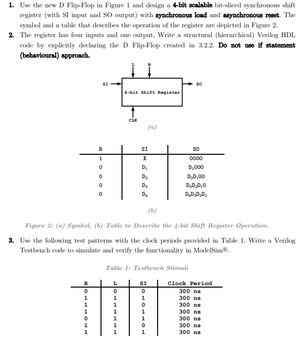
1. Use the new D Flip-Flop in Figure 1 and design a 4-bit scalable bit-sliced synchronous shift register (with SI input and SO output) with synchronous load and asynchronous reset. The symbol and a table that describes the operation of the register are depicted in Figure 2. 2. The register has four inputs and one output. Write a structural (hierarchical) Verilog HDL code by explicitly declaring the D Flip-Flop created in 3.2.2. Do not use if statement (behavioural) approach. (b) Figure 2: (a) Symbol, (b) Table to Describe the 4-bit Shift Register Operation. 3. Use the following test patterns with the clock periods provided in Table 1. Write a Verilog Testbench code to simulate and verify the functionality in ModelSim . Table 1: Testbench Stimuli
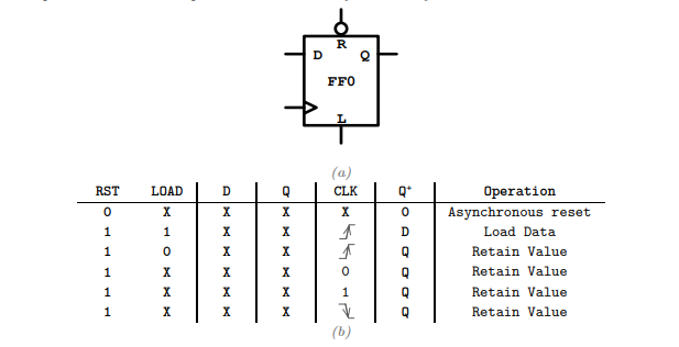
(a) \begin{tabular}{cc|c|c|c|c|c} RST & LOAD & & & & & Operation \\ \hline 0 & & & & & 0 & Asynchronous reset \\ 1 & 1 & & & A & & Load Data \\ 1 & 0 & & & & & Retain Value \\ 1 & & & & 0 & & Retain Value \\ 1 & & & & 1 & & Retain Value \\ 1 & & & & & & Retain Value \end{tabular} (b)
Expert Answer
I can help you understand how to design a 4-bit scalable bit-sliced synchronous shift register using a D flip-flop with synchronous load and asynchronous reset. I'll explain the general concept and provide a textual representation of the table you mentioned.To design a 4-bit scalable bit-sliced synchronous shift register, you can use four instances of the D flip-flop (DFF) with additional control logic for synchronous loading and asynchronous resetting. The shift register will have a serial input (SI) and a serial output (SO).The basic building block is the D flip-flop with an asynchronous reset (R) and a synchronous load (LOAD) control. The DFF has three inputs: D (data input), CLK (clock input), and RST (reset input). It also has two outputs: Q (output) and Q* (complementary output). The DFF stores the value of D and updates its output Q on the rising edge of the clock (CLK) signal.To implement the 4-bit shift register, you need to connect four DFFs in series, with each DFF representing one bit of the register. The Q output of each DFF feeds into the D input of the next DFF, creating a shift register structure.Now, let's describe the operation of the register using a table:In the table:CLK represents the clock input.RST represents the asynchronous reset input. When RST is 0, it resets all the flip-flops to 0.LOAD represents the synchronous load input. When LOAD is 1, the input value (SI) is loaded into the shift register on the rising edge of the clock.SI represents the serial input. It is the value to be loaded or shifted into the shift register.Q3, Q2, Q1, and Q0 represent the outputs of the four DFFs, representing the four bits of the shift register.SO represents the serial output. It is the output of the least significant bit (Q0).Please note that X represents "don't care" values, and the table assumes positive-edge triggering for the clock input (CLK).With this table, you can implement the behavior of the 4-bit scalable bit-sliced synchronous shift register using the new D flip-flop provided.