Home /
Expert Answers /
Electrical Engineering /
a-schematic-of-a-loaded-bjt-3c2bjt1-inverter-is-shown-below-driving-a-load-modelled-by-the-resi-pa240
(Solved): A schematic of a loaded, BJT (3C2BJT1) inverter is shown below, driving a load modelled by the resi ...
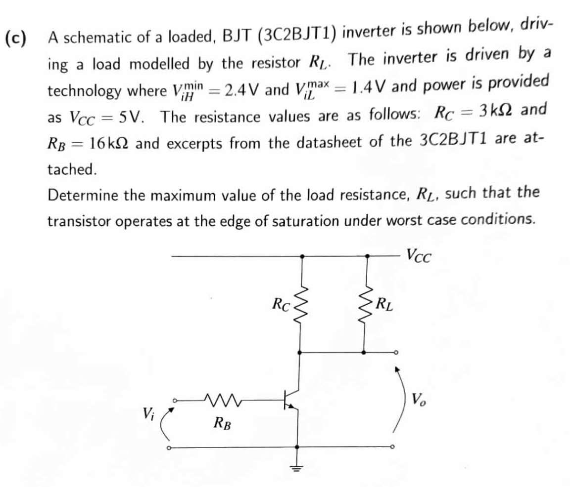
A schematic of a loaded, BJT (3C2BJT1) inverter is shown below, driving a load modelled by the resistor \\( R_{L} \\). The inverter is driven by a technology where \\( V_{i H}^{\\min }=2.4 \\mathrm{~V} \\) and \\( V_{i L}^{\\max }=1.4 \\mathrm{~V} \\) and power is provided as \\( V_{C C}=5 \\mathrm{~V} \\). The resistance values are as follows: \\( R_{C}=3 \\mathrm{k} \\Omega \\) and \\( R_{B}=16 \\mathrm{k} \\Omega \\) and excerpts from the datasheet of the 3C2BJT1 are attached. Determine the maximum value of the load resistance, \\( R_{L} \\), such that the transistor operates at the edge of saturation under worst case conditions.