Home /
Expert Answers /
Electrical Engineering /
a-rs-latch-is-shown-below-with-its-input-output-truth-table-draw-its-gate-diagram-using-two-inv-pa580
(Solved): (a) RS latch is shown below with its input-output truth table. Draw its gate diagram using two inv ...
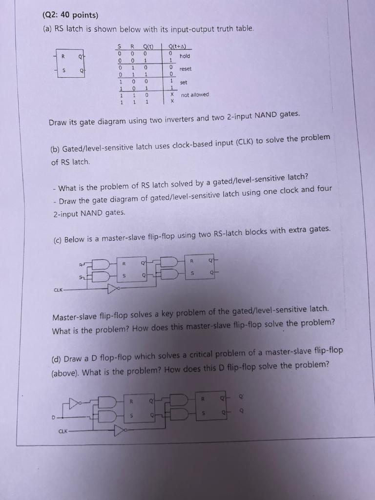
(a) RS latch is shown below with its input-output truth table. Draw its gate diagram using two inverters and two 2 -input NAND gates. (b) Gated/level-sensitive latch uses clock-based input (CLK) to solve the problem of RS latch. - What is the problem of RS latch solved by a gated/level-sensitive latch? - Draw the gate diagram of gated/level-sensitive latch using one clock and four 2-input NAND gates. (c) Below is a master-slave flip-flop using two RS-latch blocks with extra gates. Master-slave flip-flop solves a key problem of the gated/level-sensitive latch. What is the problem? How does this master-slave flip-flop solve the problem? (d) Draw a D flop-flop which solves a critical problem of a master-slave flip-flop (above). What is the problem? How does this D flip-flop solve the problem?