Home /
Expert Answers /
Electrical Engineering /
a-calculate-the-maximum-operating-frequency-of-the-circuit-shown-in-figure-q3-1-the-registers-h-pa319
(Solved): (a) Calculate the maximum operating frequency of the circuit shown in Figure Q3.1. The registers h ...
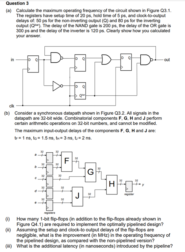
(a) Calculate the maximum operating frequency of the circuit shown in Figure Q3.1. The registers have setup time of \( 20 \mathrm{ps} \), hold time of \( 5 \mathrm{ps} \), and clock-to-output delays of: \( 50 \mathrm{ps} \) for the non-inverting output (Q) and \( 80 \mathrm{ps} \) for the inverting output ( \( \left.Q^{\text {bar }}\right) \). The delay of the NAND gate is \( 200 \mathrm{ps} \), the delay of the OR gate is \( 300 \mathrm{ps} \) and the delay of the inverter is \( 120 \mathrm{ps} \). Clearly show how you calculated your answer. (b) Consider a synchronous datapath shown in Figure Q3.2. All signals in the datapath are 32-bit wide. Combinatorial components \( \mathbf{F}, \mathbf{G}, \mathbf{H} \) and \( \mathbf{J} \) perform certain arithmetic operations on 32-bit numbers, and cannot be modified. The maximum input-output delays of the components \( \mathbf{F}, \mathbf{G}, \mathbf{H} \) and \( \mathbf{J} \) are: \( \mathrm{t}_{\mathrm{F}}=1 \mathrm{~ns}, \mathrm{t}_{\mathrm{G}}=1.5 \mathrm{~ns}, \mathrm{t}_{\mathrm{H}}=3 \mathrm{~ns}, \mathrm{t}_{\mathrm{J}}=2 \mathrm{~ns} \). (i) How many 1-bit flip-flops (in addition to the flip-flops already shown in Figure Q4.1) are required to implement the optimally pipelined design? (ii) Assuming the setup and clock-to output delays of the flip-flops are negligible, what is the improvement (in \( \mathrm{MHz} \) ) in the operating frequency of the pipelined design, as compared with the non-pipelined version? (iii) What is the additional latency (in nanoseconds) introduced by the pipeline?
Expert Answer
Given setup time = 20ps hold time = 20ps clk-to-q = 50ps clk-to-q' = 80ps NAND = 200p