Home /
Expert Answers /
Electrical Engineering /
3-draw-the-schematic-of-a-multiplier-circuit-using-long-multiplication-that-multiplies-ab-w-pa837
(Solved): 3. Draw the schematic of a multiplier circuit using long multiplication, that multiplies AB, w ...


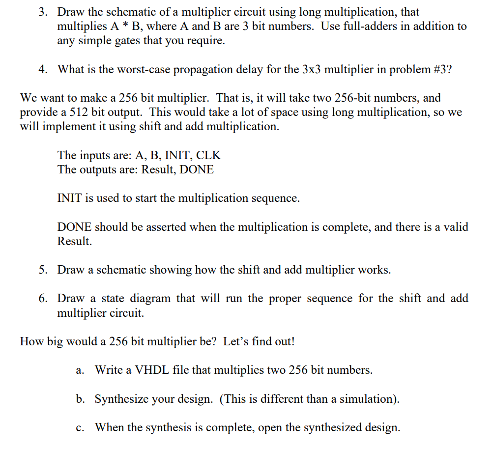
3. Draw the schematic of a multiplier circuit using long multiplication, that multiplies , where and are 3 bit numbers. Use full-adders in addition to any simple gates that you require. 4. What is the worst-case propagation delay for the multiplier in problem \#3? We want to make a 256 bit multiplier. That is, it will take two 256-bit numbers, and orovide a 512 bit output. This would take a lot of space using long multiplication, so we will implement it using shift and add multiplication. The inputs are: A, B, INIT, CLK The outputs are: Result, DONE INIT is used to start the multiplication sequence. DONE should be asserted when the multiplication is complete, and there is a valid Result. 5. Draw a schematic showing how the shift and add multiplier works. 6. Draw a state diagram that will run the proper sequence for the shift and add multiplier circuit. How big would a 256 bit multiplier be? Let's find out! a. Write a VHDL file that multiplies two 256 bit numbers. b. Synthesize your design. (This is different than a simulation). c. When the synthesis is complete, open the synthesized design.
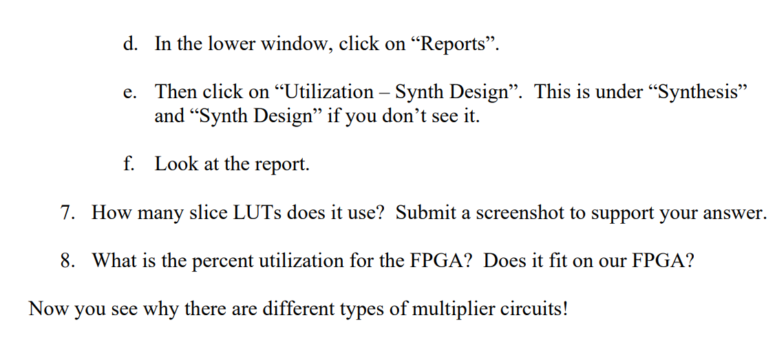
d. In the lower window, click on "Reports". e. Then click on "Utilization - Synth Design". This is under "Synthesis" and "Synth Design" if you don't see it. f. Look at the report. 7. How many slice LUTs does it use? Submit a screenshot to support your answer 8. What is the percent utilization for the FPGA? Does it fit on our FPGA? Now you see why there are different types of multiplier circuits!