Home /
Expert Answers /
Advanced Math /
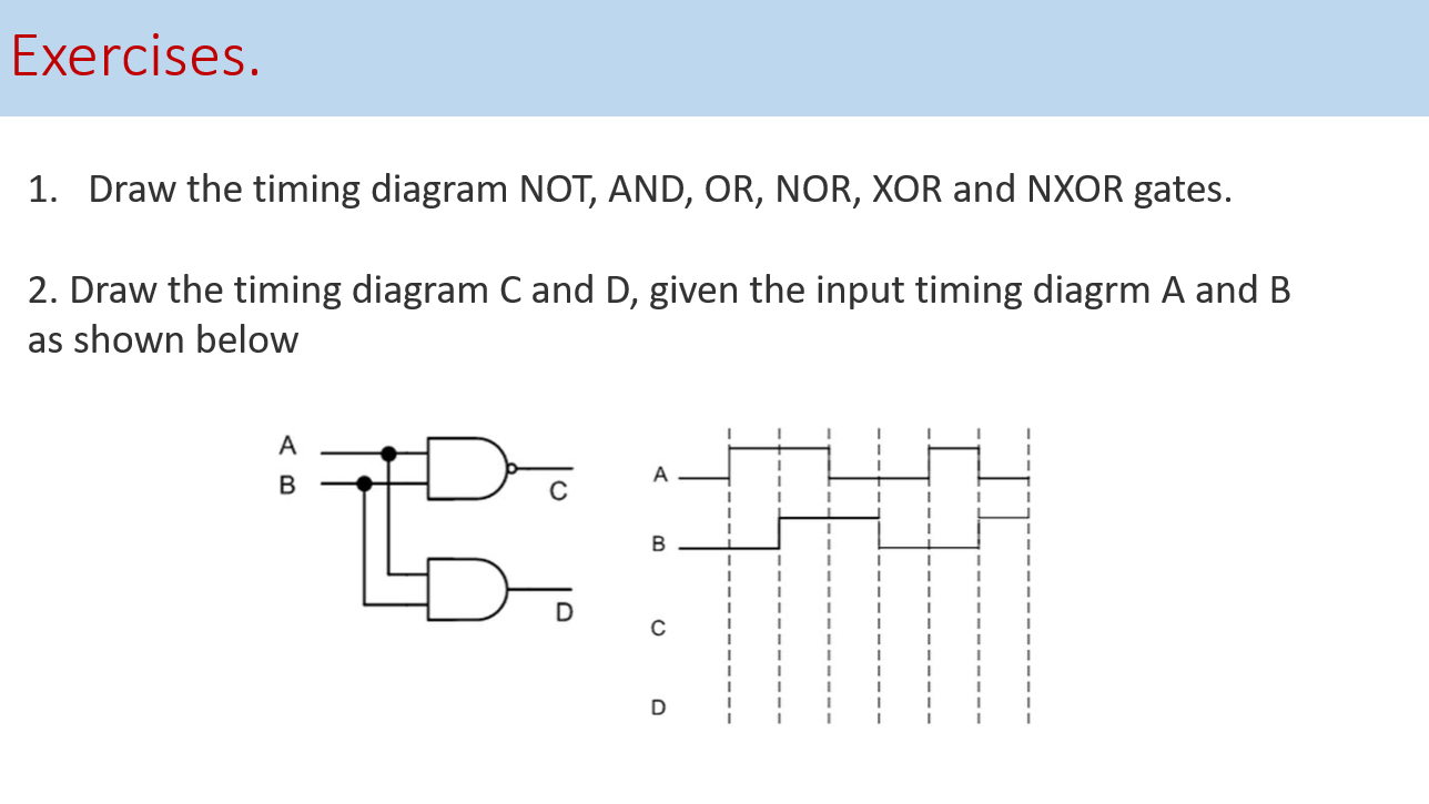
1-draw-the-timing-diagram-not-and-or-nor-xor-and-nxor-gates-2-draw-the-timing-diagram-c-and-pa379
Expert Answer
1. Timing diagram of NOT, AND, OR, N
